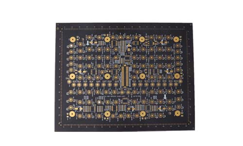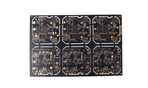
Die Die 6-lagige LED-Leiterplatte mit kleinem Rastermaß erster Ordnung ist eine Hochleistungsleiterplatte, die für LED-Bildschirme mit extrem hoher Anzeigegenauigkeit und hervorragender Wärmeableitungsleistung entwickelt wurde.
6-layer One-stage Led Small-pitch Display PCB Board Product Introduction
 |
 |
1.Produktübersicht
The 6-layer first-order LED small pitch display PCB circuit board is a high-performance circuit board designed for LED display screens with extremely high display accuracy and excellent heat dissipation performance. This product is widely used in advertising media, performances, conference rooms, shopping malls and other places, and can achieve high-definition image and video display.
2.Produktmerkmale
Small pitch design:
Adopting small pitch LED technology, the pitch is usually between 1.0mm and 3.9mm, which can provide more delicate image display effects and is suitable for close viewing.
High resolution:
Support high-resolution display, which can meet the needs of ultra-high-definition display such as 4K and 8K, ensuring clear images and bright colors.
6-layer PCB design:
Adopting a 6-layer PCB structure, the stability and reliability of the circuit are enhanced, while effectively reducing electromagnetic interference and improving signal transmission quality.
Hervorragende Wärmeableitungsleistung:
Adopt high thermal conductivity materials and reasonable layout design to optimize the heat dissipation channel, ensure that the LED lamp beads can maintain a good working temperature at high brightness and extend the service life.
Flexible installation method:
The design meets modular standards, is easy to install and maintain, and supports a variety of installation methods, such as wall hanging, bracket, etc.
Strong anti-interference ability:
After strict EMI and ESD testing, it has good anti-interference ability and is suitable for working in complex electromagnetic environments.
3. Technische Parameter
| Number of layers | 6 | Mindestlinienbreite und Zeilenabstand | 0.1/0.1mm |
| Board thickness | 1,6 mm | Minimale Blende | 0,2 |
| Board material | BT material | Oberflächenbehandlung | 2U” immersion gold |
| Kupferdicke | 1oz inner layer and 1OZ outer layer | Process points | 6-layer first-order HDI + 120,000 test points/PCS |
4. Anwendungsfeld
Werbemittel: Werbeanzeige an öffentlichen Orten wie Einkaufszentren, Straßen und Bahnhöfen
Aufführungsaktivitäten: Live-Events wie Konzerte, Ausstellungen und Konferenzen
Innen- und Außendisplay: LED-Display in Stadien, Messezentren und anderen Orten
Monitoring system: information display in security monitoring centers
 |
 |
5. Fazit
The 6-layer first-order LED small-pitch display PCB circuit board has become an indispensable part of modern display technology with its excellent display effect, stable performance and flexible application. Whether in commercial display or public information dissemination, it can provide an excellent visual experience. We are committed to providing customers with high-quality products and services to meet the needs of various industries.
FAQ
Q: Can you make HDI PCB substrates?
A: We can achieve any interconnection of 18 layers of HDI from the fourth order to the first order.
F: Wie viele Mitarbeiter haben Sie in Ihrer Fabrik?
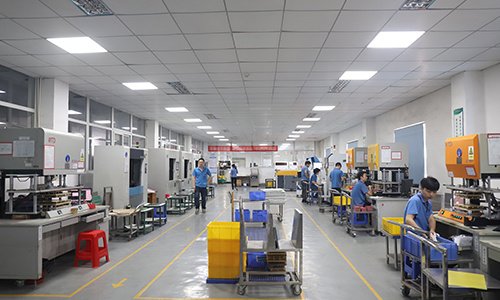
A: 500 + people
F: Sind die verwendeten Materialien umweltfreundlich?
A: Die verwendeten Materialien entsprechen den ROHS- und IPC-4101-Standards.
Q: How to solve the heat dissipation problem of small-pitch PCB circuit boards?
A: Heat dissipation mainly depends on thermal conductive materials, and the thickness of copper foil is also very important. Too thick will affect the cost, and too thin will affect the heat dissipation effect.
Q:What about the short circuit problem?
A: This is mainly caused by poor welding. The welding temperature and time must be strictly controlled. In addition, check whether there are dangling solder joints in the design.
Q:How to ensure signal integrity?
A: The key lies in reasonable layout, avoiding long-distance signal lines, and paying attention to line width and impedance matching.